My 6809 Design of 1990
(Or: How to build a small computer on a budget, and
lessons I learnt on how to actually make it work)
I built this single board computer in 1990, while I was studying
at the University of Stellenbosch. I used smARTWORK to design the
double-sided, NON-through-hole-plated PCB. The biggest plotter
I could easily get my hands on was an A3 model, and this defined
the maximum size of the PCB (plotting in 2:1, of course, and allowing
for margins etc.)
The design fits the following on a 140x80 mm PCB:
![[Image] Homebrew 6809](../ccc/images/6809s.jpg)
|
- 68B09E processor (left over from
my previous design,
otherwise I would have used the standard 6809, which does not require
the external quadrature clocks)
- 2 x 32K RAM (giving 64K total)
- 32K EPROM
- 6850 ACIA (serial port)
- MAX232 for above
- 6522 VIA
- Processor clock, reset, address decoding, baud rate generator.
|
Unfortunately I could never get this thing to work. And somewhere
along the way I reversed the power, or put 12V on the board,
or something, blowing most of the chips, so, again, this board
was sidelined.
So, now we come to 2001, where I clean out my shack, rediscover
my 6809 computer, and start investigating.
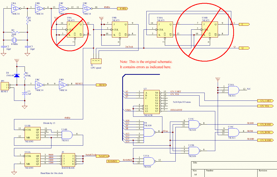
Error the first: the quadrature clock
Of course, I have learnt a lot over the past 10 years, so this
time I don't just plug all the components in and hope it works.
First, just the 74HC14 which is the oscillator. No clock. But
a replacement 74HCT04 works. So the 74HC14 was one of the casualties...
OK, plug in the 74HC73 flip-flop that generates the quadrature
clock. And use a scope (did I mention I have better tools available
nowadays? :-) to determine that, oops, Q is lagging E (the
datasheet shows that Q should lead E) -- Hmmm, that explains
why the thing never worked, I checked for clocks but I didn't
have a scope then to check for phase. Also, the clock is at
500 kHz instead of 1 MHz.
The circuit I used to generate the clocks comes from a pretty
official looking document ("Motorola Microcomputers
M6809 Course Outline") which is dead wrong. (The schematic
in the 6809E datasheet is right, but obviously I did not have
a copy of that available at the time).
As you can see from the schematic, the address decoding is, well, to
say the least, interesting. This would of course have been a lot
easier with a PAL, but I didn't have access to the PAL tools
at the time.
A15 selects the bottom 32K block of RAM. As such, there is always
RAM from $0000 to $7FFF. U6, an eight input NAND gate, maps the
top 256 bytes of address space ($FF00-$FFFF) as I/O space, which
is further decoded by a 74LS138 to form 8 blocks of 32 bytes
each. The top one of these blocks always selects the ROM, so
there is always ROM mapped from $FFE0-$FFFF. Now for the
tricky bit... depending on the state of an output pin from
the VIA, the rest of memory ($8000-$FEFF) will be either
RAM or ROM. The idea is, of course, to boot from ROM and to
then map the ROM out and the RAM in.
2002-09-16: It lives! I replaced most of the chips (RAM
and ACIA was fine, 6809 was blown though) and put a scope on
the address and data lines, alright!
I wrote some test code to access the I/O areas, basically:
	;****************************************************
	;*            Test code 2002-09-16
	;****************************************************

        .org 0xf000
reset:
        ; access all the peripherals in the system and loop

        ldaa acia

        ldaa via
        ldaa via

        ldaa io2
        ldaa io2
        ldaa io2

... and so forth for all 7 I/O areas ...

        jmp reset
Well, that worked as expected. Plugged in the ACIA and an EPROM
with DEBUG09 which I had edited way-back-when to sit at $F000-$F7FF
and to use "my" ACIA address, and hey, I get characters coming
out of the ACIA. Looks promising, except that the ACIA continuously
sends NULLs. (It does look as if it's sending the startup message first,
though).
2002-09-17: Live and learn. The AVMA signal on the 6809E is
not the same as the VMA signal on 6800 machines. So address
decoding circuits should not use it to determine when a memory
access is valid (basically, it halves the time available for the
peripheral or memory to respond to the access cycle). I tied pin 6
of the 74LS138 high, and things are looking up.
Error the second: the baud rate generator
To generate the ACIA clocks, I divided the 4MHz clock by 13,
and then by 2, 4, 8 and 16 to get 9600, 4800, 2400 and 1200
baud (16x divider in the ACIA).
Well, the circuit I used does not work. I used a 74LS393 ripple
counter, with a three input AND gate to reset the counter when
a count of "1101" is reached. In theory, this should work. In
practice, the 74LS393 is a ripple counter, meaning that
the outputs don't all change state at the same time, meaning that
strange things can, and do, happen.
A synchronous counter would have worked fine. So would
using a presettable counter like the 74LS161 counting up
from 3 (connect load to carry via an inverter).
Disappointed?
If you came here looking for a well designed 6809 computer, well,
this isn't it. Rather look at
Frank Wilson's design, which is complete
and well documented. If you came here to learn, I hope you did :-)
![[Image] Homebrew 6809](../ccc/images/6809.jpg)